
1 — Background: What the RM06F7501CT 0603 SMD resistor is and why failures matter
1.1 — Part basics & typical use cases
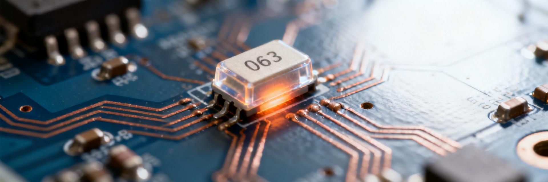
The RM06F7501CT is an 0603-format chip resistor commonly used for pull-ups, sense resistors, damping, and small current paths. 0603 SMD resistor parts in this class typically range in power handling near 1/10–1/16 W at recommended derating and have standard tolerances (e.g., 1%–5%) depending on specifications. Understanding package limits and board roles helps prioritize tests—sense resistors directly affect measurements, whereas pull-ups affect digital logic levels. Consequently, a single failed resistor can have an outsized impact on overall system performance.
1.2 — Field impact of resistor failures
Resistor faults present as open circuits, value drift, intermittency, or thermal damage, causing diverse system-level symptoms. Field reports show functional failures, increased noise floors, calibration drift, and localized overheating tied to resistor faults. Catching these failure patterns early shortens debug time. For example, a drifting sense resistor will shift ADC readings, while a cracked termination may act as an intermittent open under vibration. Targeted in-circuit checks are critical to prevent lengthy isolation cycles.
2 — Data analysis: Frequency & conditions of observed failures
2.1 — Failure-rate breakdown by cause
Failures distribute across soldering, thermal, mechanical, and intrinsic drift causes. Typical breakdowns observed in lab and field diagnostics often fall into specific bands: solder joint defects (30–45%), thermal overstress (15–30%), value drift or resistor element degradation (10–20%), and mechanical damage/tombstoning (10–20%). Where exact internal numbers are lacking, hardware teams should instrument reflow and post-build inspection data to quantify local ranges and prioritize corrective actions.
| Failure Cause | Typical Range |
|---|---|
| Solder joint defects | 30–45% |
| Thermal overstress / burn | 15–30% |
| Value drift / element degradation | 10–20% |
| Mechanical damage / tombstoning | 10–20% |
2.2 — Environmental and process correlations
Failures correlate strongly with reflow peaks, multiple reflow cycles, board thermal mass imbalances, and handling/cleaning processes. Assemblies with high thermal gradients, excessive peak temperatures, or repeated reflows show higher thermal overstress and solder joint cracking rates. Aggressive solvent exposure or poor conformal coating adhesion increases corrosion-related drift. Engineering teams must monitor reflow profile logs, peak temperatures, and cycle counts, correlating this data with returned-unit diagnostics to confirm causal links before implementing permanent fixes.
3 — Failure patterns: visual, electrical, and microscopic symptoms
3.1 — Electrical signatures and quick bench tests
Quick electrical checks narrow suspects rapidly. Expected healthy resistance equals the nominal value within tolerance (7.5kΩ for the RM06F7501CT). Opens read as OL or very high megohms, and drift shows percent deviation under load. Apply the following standard bench verification sequence:
- Measure in-circuit resistance with a high-accuracy multimeter—note deviation versus nominal.
- Check continuity and voltage drop under a controlled, set current to detect internal intermittency.
- Run an IR thermal scan during functional testing to locate hot-running resistors and uneven thermal distribution.
- Desolder and measure out-of-circuit if parasitic paths obscure the readings.
3.2 — Visual & microscopic indicators
Visual cues often reveal the root cause without invasive testing. Common indicators include cracked or lifted terminations, dull or insufficient fillets, tombstoning, blackened ceramic bodies from thermal burn, thin-film delamination, and characteristic flux residue patterns that indicate wetting issues. Photograph suspects at oblique and top-down angles using 20x to 50x magnification to document termination cracks and pad wetting; these images accelerate cross-team process analysis.
4 — Fixes & rework procedures: from quick repairs to root-cause corrections
4.1 — Safe rework steps for 0603 resistors
A controlled rework sequence minimizes collateral damage to adjacent components. Technicians following this standard flow report higher first-pass repair success:
- Preheat the local board area (~100–120°C) and apply a small drop of low-residue tacky flux. Use a targeted hot-air nozzle (2–3 mm diameter).
- Remove the failed part using micro-tweezers or dual-iron tips to avoid trace tearing; clean pads gently using flux remover and copper braid.
- Inspect the copper pads for lifted traces. Apply fresh solder paste or wire solder, place the replacement component, reflow, and inspect solder fillets.
- Verify the connection in-circuit and thermally inspect the board under operational load.
4.2 — Corrective fixes for root causes
Fixes must match the specific root cause to prevent recurrence. Standard process modifications include:
- Solderability issues: Revise the solder paste chemistry, stencil aperture design, or pad finish (e.g., transition to ENIG).
- Thermal overstress: Lower reflow peak temperatures, optimize the soak profile, or specify a higher power-rated part.
- Mechanical cracking: Adjust pad geometries, add solder-mask fillets, or improve board support during handling/depanelization.
- Tombstoning: Balance copper trace routing to equalize heat sinking on both pads, and optimize pick-and-place nozzle alignment.
5 — Case study + quick checklist for field technicians
5.1 — Short case study
- Symptom: Intermittent ADC offset errors detected on a series of sensor boards; visual inspection showed one RM06F7501CT resistor with an incomplete fillet.
- Diagnosis: In-circuit resistance check fluctuated under physical board vibration. Microscopy revealed insufficient solder paste volume on one pad (a tombstone precursor).
- Fix & Outcome: Adjusted stencil aperture geometries to increase solder paste volume on thermal-relief pads and reworked the affected resistors. Post-fix vibration tests passed cleanly and field returns dropped to zero for that lot.
5.2 — Actionable field checklist & prevention tips
- Inspect all terminations for micro-cracking, dull fillets, or voids under 20x magnification.
- Measure actual resistance values; perform real-time IR scans for localized hotspots.
- Reflow and rework strictly per standard operating procedures; avoid multiple reheats on adjacent 0603 passives.
- Preventive Action: Review stencil apertures, pick-and-place force, and reflow profiles during routine process audits.
Key summary
- Most common failure patterns for this family include solder joint defects, thermal overstress, value drift, and mechanical damage; rapid in-circuit testing and IR inspection narrow suspects quickly and guide targeted rework.
- Practical fixes range from controlled rework (preheat, flux, hot-air) to process changes—stencil/paste adjustments, reflow-profile tuning, pad geometry updates—and verification via thermal cycling or x-ray when needed.
- Field checklist: document visual signs, measure resistance, limit reheats, adjust process parameters, and escalate intermittents to lab; these steps reduce return rates and time-to-repair for 0603 SMD resistor issues.
Summary
In summary, RM06F7501CT failures typically present as opens, value drift, solder/joint cracking, or thermal damage, each requiring distinct diagnostic and corrective approaches. Combining visual, electrical, and process data rapidly reveals root causes, while process fixes—stencil, paste, reflow profile, and pad design—prevent recurrence. Apply the quick checklist and verification steps outlined here to reduce MTTR and improve field reliability for these 0603 SMD resistor failure patterns.
Common questions and answers
How do I quickly verify an RM06F7501CT on a suspect board?
Use a focused sequence: document visual appearance, measure in-circuit resistance with a calibrated meter, apply a known test current and measure voltage drop, and perform a brief IR scan under functional load. If results are ambiguous, remove the part and measure out-of-circuit; this isolates board parasitics and confirms whether the resistor itself has drifted or failed.
What are the telltale signs of a failing 0603 SMD resistor under microscopy?
Under 20–50x magnification, look for cracked or lifted terminations, uneven or missing solder fillets, body blackening from thermal events, and substrate delamination. Flux residue patterns that show poor wetting or voids at one termination often precede tombstoning; photographic documentation helps correlate with process records for corrective action.
Which reflow profile changes reduce thermal overstress for 0603 SMD resistor assemblies?
Lowering peak temperature, reducing time above liquidus, and smoothing thermal ramps reduce component thermal stress; also minimize the number of reflow passes. Evidence-driven adjustments require comparing reflow logs to board thermal mass and verifying solder joints post-change, then running a short thermal cycle test to confirm improved reliability.
What physical mechanism causes tombstoning in 0603 components during reflow?
Tombstoning is driven by surface tension imbalance when solder paste on one pad melts before the other. This occurs due to uneven track thermal masses, asymmetric pad dimensions, or slight component misalignment, pulling the chip upright into a vertical position.